
Case Studies
Read about some of our current and past projects to discover how working with Coventry University could benefit your business.

HORIBA MIRA
A global leader in advanced vehicle engineering, research and product testing, wanted to develop new key technologies and skills that were needed in the business to achieve measurable impact.
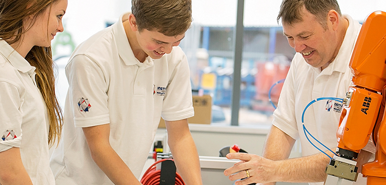
Unipart Manufacturing
Learn how we successfully combined the best in academia, industry and R&D into a real-world environment through the creation of a specialist institute and the UK's first 'Faculty on the Factory Floor'.

KPIT Technologies
We have partnered with India-based KPIT Technologies for the delivery of approved postgraduate programmes providing employees with vital perspectives of innovation, sustainability and organisational objectives.

SEL Environmental
A KTP between SEL Environmental and the University’s Centre for Agroecology and Water Resilience (CAWR) to deliver the benefits of green space and wildlife-friendly habitats into the heart of urban areas.

Stevenage Circuits
Read about a a 2-year KTP project to improve manufacturing capability to meet the future requirements for high reliability military-aerospace grade HDI printed circuit boards.
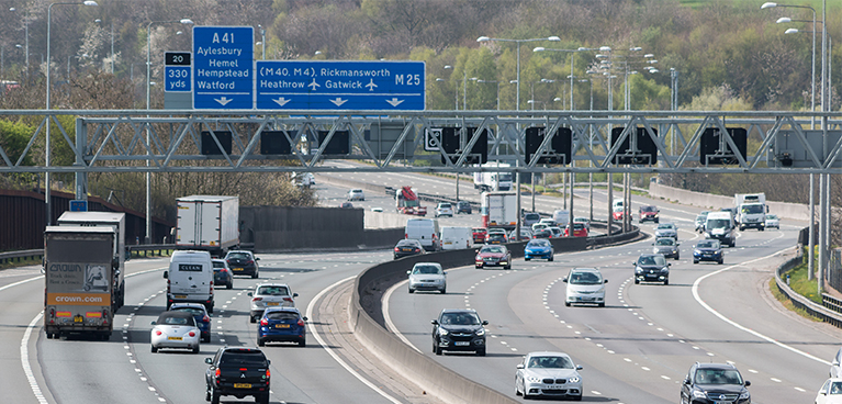
Highways England
Working with the company that oversees the maintenance and improvement of the UK's motorways and major A roads, to develop and deliver bespoke leadership training.

Life Science Group
Biomedical science experts are working with industry to develop new products to conform to new legislation, prevent contamination and allow reproducibility.

ITP Group
University metrology experts work to develop a new multi-coordinate control and measuring system for large machines.

CyberOwl
Cyber security specialists at Coventry University in partnership with industry counterparts have created a new commercial venture to tackle cyber threats.
For more information please Contact Us


